
离岸价格
Get Latest Price|
- Minimum Order
国:
China
モデル番号:
-
离岸价格:
ロケーション:
-
最低注文量の価格:
-
最低注文量:
-
パッケージの詳細:
-
納期:
-
供給能力:
-
支払いタイプ:
-
製品グループ :
連絡先担当者 Tracy
Shenzhen, Guangdong
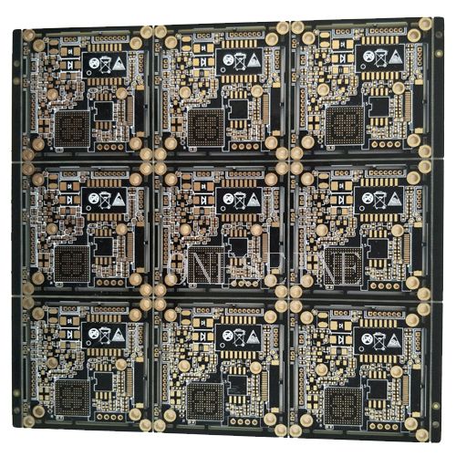
8 Layer Gold Plated PCB Multilayer Printed Circuit Boards
Fabrication
PCB information:
Material: FR4 3 core ,6 layers,fake 8 layers
Surface finish:Gold plated
Copper weight:2OZ
Color: Black and white silkscreen
Board size:6*6cm
Stack up layer information as follow:
NO.1
1 Signal 1 component side, microstrip trace layer
2 Signal 2 internal microstrip trace layer, better trace layer (X
direction)
3 Ground
4 Signal 3 stripline routing layer, better trace layer (Y
direction)
5 Signal 4 Stripline Layer
6 Power
7 Signal 5 Internal Microstrip Trace Layer
8 Signal 6 Microstrip Trace Layer
NO.2
1 Signal 1 component SIDE, microstrip trace layer, good trace
layer
2 Ground layer, better electromagnetic wave absorption capacity
3 Signal 2 stripline routing layer, good routing layer
4 Power power layer, and the underlying stratum constitute
excellent electromagnetic absorption
5 Ground layer
6 Signal 3 stripline routing layer, good routing layer
7 Power Formations with Large Power Supply Impedance
NO.3
This is not a good way to stack boards due to poor electromagnetic
absorption capability and large power supply impedance. Structure
as follows:
1 Signal 1 component side, microstrip trace layer
2 Signal 2 internal microstrip trace layer, better trace layer (X
direction)
3 Ground
4 Signal 3 stripline routing layer, better trace layer (Y
direction)
5 Signal 4 Stripline Layer
6 Power
7 Signal 5 Internal Microstrip Trace Layer
8 Signal 6 Microstrip Trace Layer
NO.4
It is a variant of the third stacking mode. Since the reference
layer is added and the EMI performance is better, the
characteristic impedance of each signal layer can be well
controlled.
1 Signal 1 component side, microstrip trace layer, good trace
layer
2 Ground formation, better electromagnetic wave absorption
capacity
3 Signal 2 stripline routing layer, good routing layer
4 Power power layer, and the underlying stratum constitute
excellent electromagnetic absorption
5 Ground
6 Signal 3 stripline routing layer, good routing layer
7 Power layer with Large Power Supply Impedance
Skype: oneseine-sales
| 国: | China |
| モデル番号: | - |
| 离岸价格: | Get Latest Price |
| ロケーション: | - |
| 最低注文量の価格: | - |
| 最低注文量: | - |
| パッケージの詳細: | - |
| 納期: | - |
| 供給能力: | - |
| 支払いタイプ: | - |
| 製品グループ : | HF PCB |