Shanghai,Shanghai,China China
The company is composed of a group of experienced industry experts and sales consultants, with over *0 years average experience. Relying on a number of shareholding and strategic cooperation factories, BonTek is capable of conducting collaborative research and development with customers. We are committed to providing global customers with high quality microelectronic materials, as well as supporting the construction of 5G network infrastructure and the ecological development of IoT.
Our company will continue to improve process capabilities and achieve technological breakthroughs to meet the higher requirements of customers and provide customers with sustainable core competitiveness.
今すぐお問い合わせください| ビジネスタイプ | Manufacturing |
| ウェブサイト | https://www.bon-tek.com/ |
| 設立年 | 2020 |
| 従業員数 | 16-25 |
| 主要市場 | Americas,Asia,Europe |
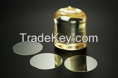
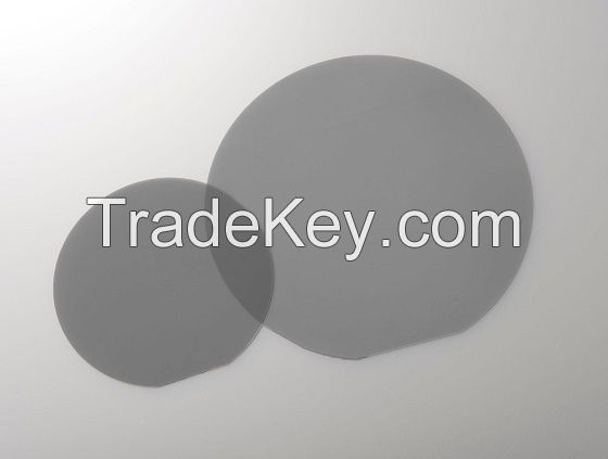
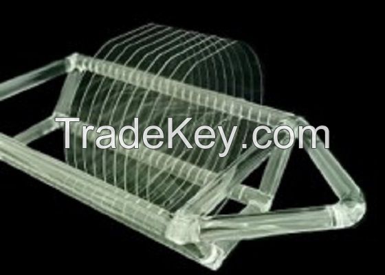
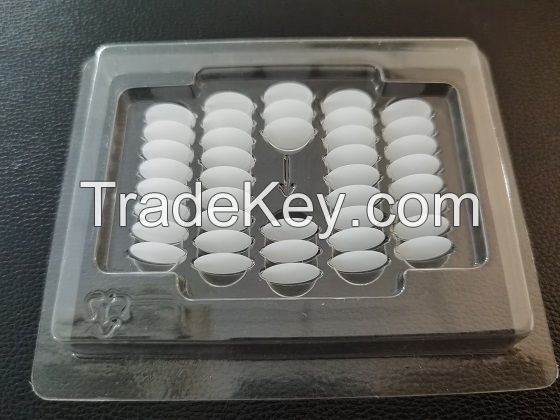
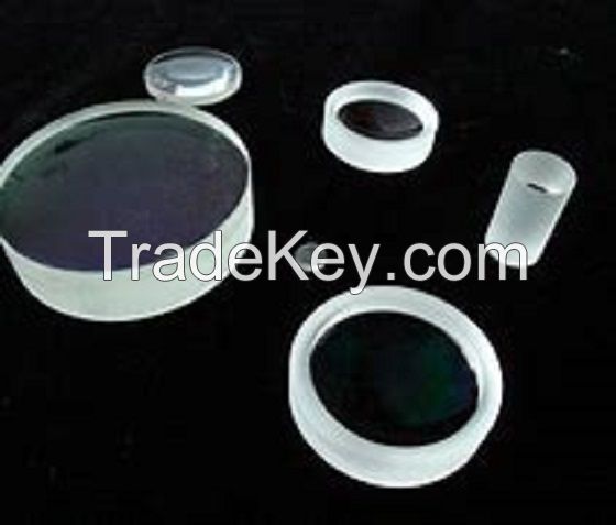
| 企業製品/サービス | lithium niobate wafer quartz crystal wafer flouride |
| 工場所在地 | Zhejiang |
| 工場サイズ | 3000 sqm to 5000 sqm |
| 生産ライン数 | 5 |
| 年間総購買量の合計 | N/A |
| 研究開発スタッフの人数 | Less than 5 people |
| 品質管理 | In House |
| 登記書 | N/A |
| 契約製造 | Design Service Offered |
| 登録資本金 | N/A |
| 所有権タイプ | N/A |
| 法定代表者/CEO | N/A |
| エクスポートパーセンテージ | N/A |
| 年間売上高合計 | N/A |
| QCスタッフの人数 | Less than 5 people |
| 連絡先担当者 | Bofan |
| 会社 | Shanghai BonTek Optoelectronic Technology Development Co., Ltd |
| 電話 | ******** |
| Mobile | ******** |
| ファックス | ******** |