Shenzhen Hengtaida Technology Co, .Ltd deals in the development and production of printed circuit boards (PCB) up to *4 layers including HDI buried via boards, Flexible printed boards (FPC) and PCB assembly (PCBA). HengtaidaTechnology Co, . Ltd was founded in ***0. The company is located in the third industrial Zoon, Fuqiao Town, Shenzhen City with the area over ***0 Square meters. We have imported the advanced facilities from US, Japan, Germany and Israel to improve our production and technical ability. We have set a great example in the PCB field of flying probe testing, buried and blind via and special controlled impedance.With the continuous effort of the R&D, we have successfully established our reputation in mechanical micro via, high density impedance and HDI.
We are always attaching great importance to the quality control and hi-tech, which are highlighted throughout all the manufacturing and after-sales process. By passing the ISO***1:***0, ISO****1:***6, TS****9, UL, our products are very popular with users.
Through the cooperation with the developed countries and customers, we have had adopted international advanced technology and management system, and we have improved our technology level from their high standard and strict quality requirements. The market system of Hengtaida is increasingly extending and scale of Hengtaida is expanding. We have profuse experience in manufacturing PCB. Our PCB daily capacity is ***0 square meters, we can deliver the SS, DS PCB sample within *4 hours, **8 layer PCB in **5 working days, for the batch quantity for double side PCB, the lead time is **5 working days, **8 layer is **8 days. The quick and fast lead time stably ensures our customer of quick research speed to occupying the market.
So far now, we have been exporting to more than *0 countries and regions like USA, U.K, the Netherlands, France, Germany, Russia, Turkey, Japan , Singapore, South Korea, South Africa and so on. Meanwhile, Such word-wide famous com
今すぐお問い合わせください
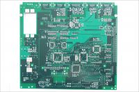 2 layer print circuit board
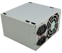 250W at power supply for Spark/Industrial/CNC machine tools
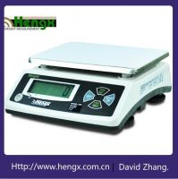 38 dollars Simple Weighing Scale
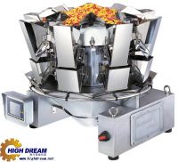 8 Heads Weigher
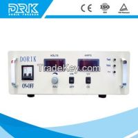 AC DC IGBT electroplating industrial switching power supply
 AC/DC Adapters
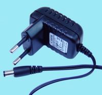 AC/DC switching adapter/charger
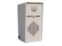 ACOUSTIC DISSUADER FOR BIRDS
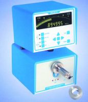 AIR ELECTRONIC AIR GAUGES, MECHANICAL AIR GAUGES,AIR GAUGE ACCESSORIES
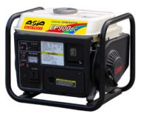 Air-cooled Portable 900 With Frame Gasoline Generator